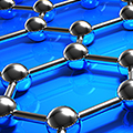
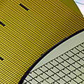
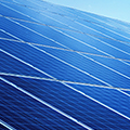
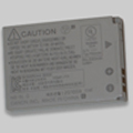
材料科学资料
资料下载:材料科学(碳、二维材料和纳米技术)
-
Application summary: Raman measurements on graphene [en]
The high specifity of inVia enables graphene to be easily differentiated from other materials, including carbon allotropes such as carbon nanotube and diamond.
-
Application note: Analyse 2D materials with the inVia Qontor confocal Raman microscope [en]
With so many unique properties, working with 2D materials can be challenging. Whether it is large regions, uneven samples, or small discrete flakes, Renishaw’s inVia Qontor confocal Raman microscope gives you reliable results, quickly and easily.
-
Product note: Rayleigh imaging using the inVia™ confocal Raman microscope [en]
Product note detailing how you can perform Rayleigh imaging on the inVia confocal Raman microscope.
资料下载:材料科学(半导体材料)
-
Application note: Photocurrent measurements on the inVia™ confocal Raman microscope [en]
When light interacts with semiconducting materials it can induce electrical currents (‘photocurrents’). These currents carry information about the electronic, optical, and charge transport properties of the material. This information is complementary to that obtainable from Raman scattering, which can identify physical changes in the material properties. This application note demonstrates the capability to simultaneously collect Raman and photocurrent data using the photocurrent mapping module concurrently with an inVia Raman microscope.
-
Application note: Analyse compound semiconductors with the inVia™ Raman microscope [en]
Over the last decade compound semiconductors have attracted a great deal of attention because they offer properties suitable for next generation devices in a wide range of application areas. Historically, the fabrication of these devices has been hindered by material challenges. While these have mainly been conquered at the research level, problems still persist when scaling up to industrial production. Renishaw’s inVia Raman microscope is a non-invasive, non-destructive characterisation tool which provides sub-micrometre information on the vibrational, crystal and electronic structure of materials.
-
Application note: Analyse silicon carbide (SiC) with the inVia Raman microscope [en]
The properties of silicon carbide are highly dependent on its crystal structure (it can exist in many polytypes), on the quality of the crystal, and on the number and types of defects present. Manufacturers of silicon carbide raw material and devices need to monitor and control these attributes to enhance yield. The first step in controlling these parameters is to measure them repeatably and quantifiably. Renishaw’s Raman systems are ideal for this.
-
News release: Identifying imperfections with Raman spectroscopy [en]
An article in Compound Semiconductor magazine, October 2015, describes how Raman spectroscopy allows routine mapping of SiC wafers in little more than an hour.
资料下载:材料科学(光伏材料)
-
Application note: Photocurrent measurements on the inVia™ confocal Raman microscope [en]
When light interacts with semiconducting materials it can induce electrical currents (‘photocurrents’). These currents carry information about the electronic, optical, and charge transport properties of the material. This information is complementary to that obtainable from Raman scattering, which can identify physical changes in the material properties. This application note demonstrates the capability to simultaneously collect Raman and photocurrent data using the photocurrent mapping module concurrently with an inVia Raman microscope.
[1.6MB] -
Poster: Simultaneous photocurrent and Raman mapping of single crystalline silicon solar cell modules [en]
A poster demonstrating the inVia's capabilities at studying the efficiency of solar cells against the quality of their manufacture.
[914kB]
下载应用说明
-
Application note: Analyse lithium-ion batteries with the inVia™ confocal Raman microscope [en]
Chemically characterise lithium-ion batteries with Renishaw’s inVia Raman microscope. inVia is the ultimate system for studies ranging from fundamental research on the materials involved through to final product quality control and failure analysis.
-
Application note: Analyse Li-ion battery anodes with the inVia™ confocal Raman microscope [en]
The inVia confocal Raman microscope is ideal for locating, discriminating, and quantifying the different forms of carbon present in anodes, even those with subtle variations in structure.
应用案例
我们有各种各样的应用案例,举例如下。
如需了解更多信息,请点击下方按钮联系当地的业务代表,并提供相应的文档编号。
文档编号 | 文档说明 |
AS001 | SEM-SCA识别钢部件上的残留物 通过立体光学显微镜观察,确定了工作抗磨损性能较差的钢部件上的疑似残留物的性质。拉曼-SEM光谱确定了残留物由包含微粒的糊剂组成,这些微粒被鉴定为金刚石(特征峰在1333 cm-1),载体糊剂为有机物质。残留物很可能是抛光剂残留。 |
AS007 | 使用不同激光激发波长的常用衬底光谱 本文档提供了制备用于拉曼分析的样品时各种常用衬底的适用性信息。有些常用衬底会带来复杂的背底,这会导致对样品拉曼谱带的解释变得复杂。因此,了解哪个选项适合给定的样品和激发波长配置是非常重要的。 |
AS026 | 研究石墨烯层间相互作用 利用带有Eclipse滤光片的inVia显微拉曼光谱仪,研究石墨烯层间相互作用和其他二维晶体,从而开创新的研究课题。 |
AS027 | 利用针尖增强拉曼光谱观察小于衍射极限的石墨烯特征 使用inVia-AFM联用系统执行针尖增强拉曼光谱 (TERS),可揭示非常详细的石墨烯信息。TERS使用特殊的等离子体针尖增大样品的局部电场,进而提高拉曼强度。 |
AS028 | 利用TERS分析单层孔雀绿 利用inVia和TERS分析微小的样品体积和微弱的拉曼散射。针尖增强拉曼光谱 (TERS) 使用特殊的等离子体针尖增大样品的电场,进而提高拉曼强度。这些针尖非常小,直径为10 nm至100 nm不等,通过利用扫描探针显微镜 (SPM) 或原子力显微镜 (AFM) 握持针尖接触样品。 |
AS030 | 石墨烯薄片的拉曼成像分析 使用StreamLine成像,快速、轻松地确定样品中石墨烯膜的层数。 |
AS033 | 定位并表征SiC中的缺陷 采用StreamLineHR 3D成像可深入了解SiC缺陷。拉曼光谱是研究SiC的强大工具。 |
AS035 | 使用inVia,呈现SiC中的多型体、应变/应力和氮浓度 使用inVia,对SiC中的多型体、应变/应力和氮掺杂进行成像。 |
AS039 | 石墨烯的拉曼测量 inVia的高特异性可以很容易区分石墨烯与其他材料,包括碳同素异性体(如碳纳米管和金刚石)。 |
AS060 | 将原位拉曼光谱与纳米压痕相结合,表征类金刚石碳 雷尼绍和Hysitron将inVia共焦显微拉曼光谱仪与TI 950 TriboIndenter联用,制备出的系统能够直接将机械性能测试与原位综合化学分析相关联。 |